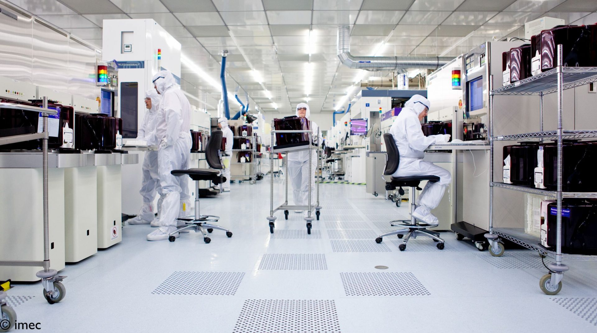
![]() Imec is an organisation with extensive clean-room facilities and other laboratory environments where a multitude of commercial as well as academic partners meet to share knowledge and instrumentation to support the further development of future nano-electronic technologies. Materials analysis is a cornerstone in the development of new technologies and 3D nanostructured devices and, as such, represents an important area where the semiconductor industry looks at imec for innovation and advanced solutions.
Imec is an organisation with extensive clean-room facilities and other laboratory environments where a multitude of commercial as well as academic partners meet to share knowledge and instrumentation to support the further development of future nano-electronic technologies. Materials analysis is a cornerstone in the development of new technologies and 3D nanostructured devices and, as such, represents an important area where the semiconductor industry looks at imec for innovation and advanced solutions.
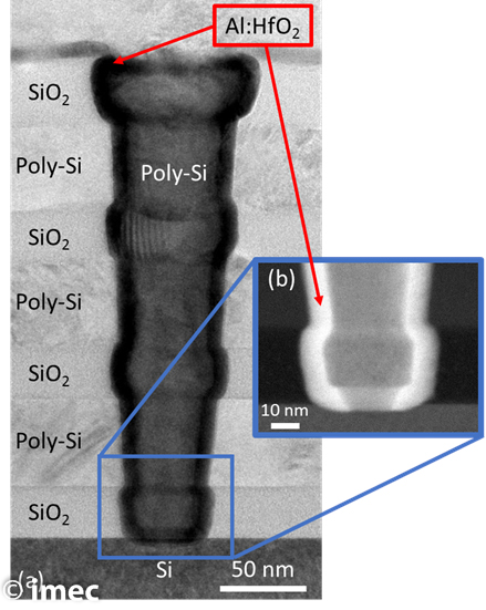
Many new processing technologies are being explored in the clean-room facilities of imec. Concurrently, metrology solutions apt to deal with ultra-thin films and 3D-structures are high in demand whereby quantification and non-destructive analysis are critical characteristics. Imec aims to set the example in exploiting high energy ion beam analysis for this purpose, e.g. through Rutherford backscattering spectrometry (RBS) and ToF-E elastic recoil detection analysis (ERD).
At Imec, we operate a 2 MV tandem accelerator (6SDH-1, NEC) and, shared with KULeuven, a 2.5 MV single-ended van de Graaf accelerator (AN2500, HVEE) to support the process developments by analyzing large volumes of samples per year and to explore new capabilities in ion beam analysis. A high capacity and efficiency is aspired through tool automation, machine learning, and multi-detector data acquisition. New capabilities and ultimate performance in terms of depth resolution and sensitivity are pursued through the exploration of novel detectors and detection schemes. Current interests are towards multi-detector RBS, high-resolution RBS using a magnetic sector and Silicon strip detector, and towards ToF-E ERD using a Gas Ionization Chamber detector. Besides, we also investigate the possibility to analyze 3D-nanostructures via ion beam analysis through 3D-tomography.
IMEC’s main areas of competence:
- materials and nanostructures for the nanoelectronics industry
- ion beam analysis
Role in RADIATE:
-
- Work package leader “Innovation, Commercial Outreach and Sustainability”
- task leader for “Innovation Management and Commercial Outreach”
- contribution to joint research activities in the advancement of detector technologies as well as in nanometrology and associated analysis
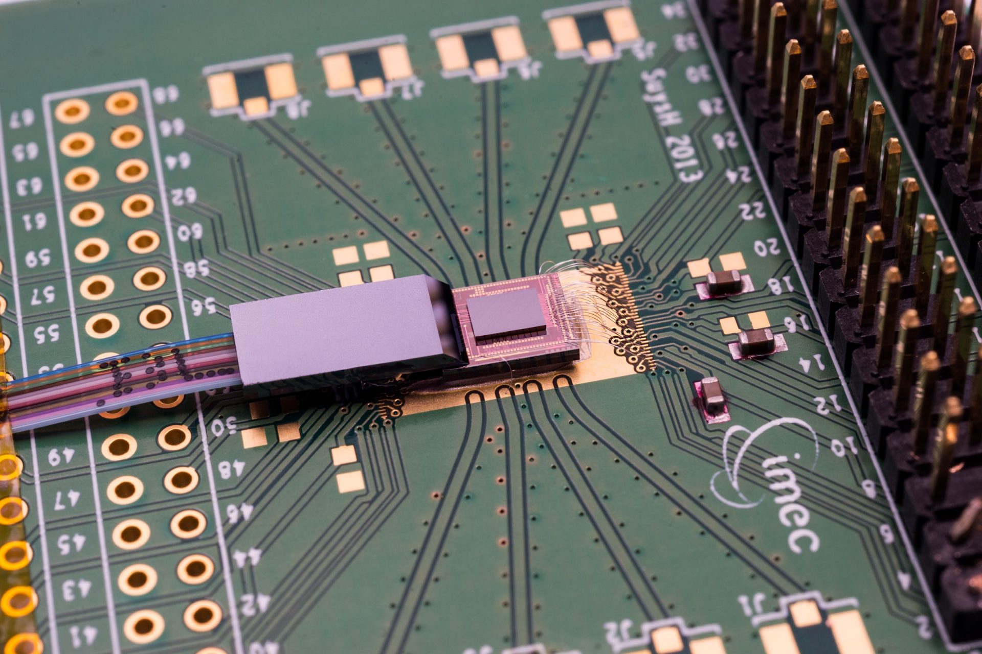
Photos: